Difference between revisions of "74HC595 8 bit Shift Register Module for Arduino"
(Created page with " == General description == This is a breakout board for 74HC595 8 bit Shift Register.The 74HCT595 are high-speed Si-gate CMOS devices and are pin compatible with Low-power S...") |
|||
| Line 1: | Line 1: | ||
== General description == | == General description == | ||
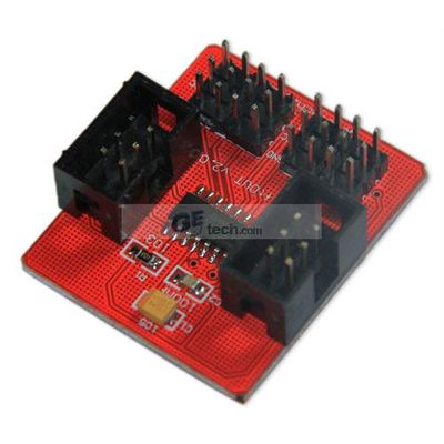
| − | + | [[File:74hc595.jpg|400px]] | |
This is a breakout board for 74HC595 8 bit Shift Register.The 74HCT595 are high-speed Si-gate CMOS devices and are pin | This is a breakout board for 74HC595 8 bit Shift Register.The 74HCT595 are high-speed Si-gate CMOS devices and are pin | ||
compatible with Low-power Schottky TTL (LSTTL). They are specified in compliance with JEDEC standard No. 7A.The 74HC595; | compatible with Low-power Schottky TTL (LSTTL). They are specified in compliance with JEDEC standard No. 7A.The 74HC595; | ||
| Line 28: | Line 28: | ||
Serial-to-parallel data conversion<br> | Serial-to-parallel data conversion<br> | ||
Remote control holding register<br> | Remote control holding register<br> | ||
| + | |||
| + | |||
| + | == Functional diagram == | ||
Revision as of 10:20, 16 March 2012
General description
 This is a breakout board for 74HC595 8 bit Shift Register.The 74HCT595 are high-speed Si-gate CMOS devices and are pin
compatible with Low-power Schottky TTL (LSTTL). They are specified in compliance with JEDEC standard No. 7A.The 74HC595;
74HCT595 are 8-stage serial shift registers with a storage register and 3-state outputs. The registers have separate
clocks.Data is shifted on the positive-going transitions of the shift register clock input (SHCP). The data in each
register is transferred to the storage register on a positive-going transition of the storage register clock input (STCP).
If both clocks are connected together, the shift register will always be one clock pulse ahead of the storage register.The
shift register has a serial input (DS) and a serial standard output (Q7S) for cascading. It is also provided with
asynchronous reset (active LOW) for all 8 shift register stages. The storage register has 8 parallel 3-state bus driver
outputs. Data in the storage register appears at the output whenever the output enable input (OE) is LOW.
Features and benefits
8-bit serial input
8-bit serial or parallel output
Storage register with 3-state outputs
Shift register with direct clear
100 MHz (typical) shift out frequency
ESD protection:
HBM JESD22-A114F exceeds 2 000 V
MM JESD22-A115-A exceeds 200 V
Multiple package options
Applications
Serial-to-parallel data conversion
Remote control holding register